Shop Talk
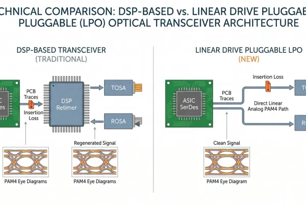
Linear Pluggable Optics: The AI Interconnect That Cuts Power Without Killing Serviceability
LPO removes the module DSP and shifts equalization to the host SerDes, cutting 800G optics toward 5.5–10 W while keeping hot-swappable QSFP-DD/OSFP cages. How analog TIAs, InP lasers, MSA specs, and China-vs-West capacity shape AI fabric demand.
read moreInside the 800G and 1.6T Optical Transceiver Bottleneck: InP, AI Fabrics, and Geopolitics
Explore the engineering, indium phosphide (InP) laser supply constraints, and geopolitical risks shaping 800G and 1.6T optical transceivers for AI data centers.
read more
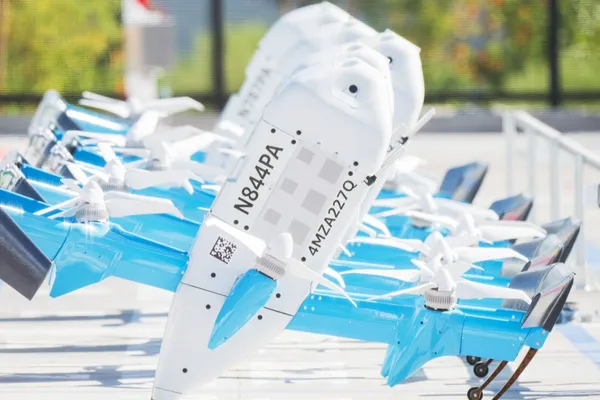
The Physics of Flight and the Economics of Scale: Drone Manufacturing Technology and Last-Mile Delivery
How the Amazon Prime Air MK30, Composite-Based Additive Manufacturing (CBAM), and BVLOS autonomy are solving the aerospace manufacturing bottleneck and last-mile unit economics.
read moreUnboxed vs. Intelligent Islands: The Two Post-Fordist Automotive Manufacturing Paradigms
Tesla’s Unboxed Assembly and China’s Intelligent Island manufacturing challenging Henry Ford’s century-old moving assembly line, diverging between hyper-volume unit cost and mixed-model agility.
read more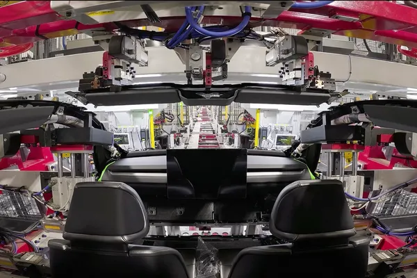
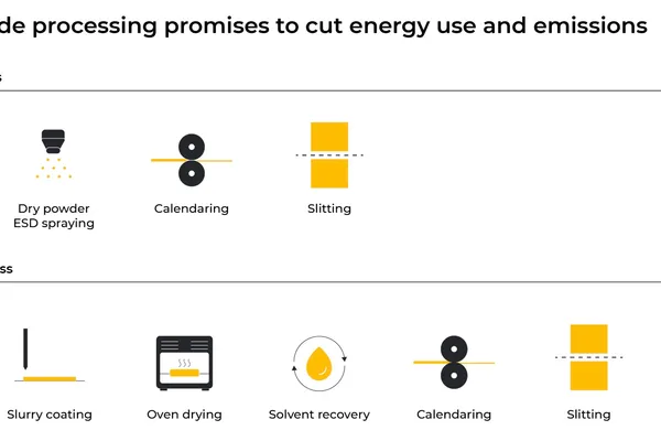
Dry Electrode Manufacturing: Eliminating Solvents, Ovens, and the Gigafactory Footprint
Dry electrode manufacturing eliminates toxic NMP solvents, 100-meter drying ovens, and binder migration, slashing gigafactory capex and unlocking solid-state cells.
read moreHow Autonomous Labs Turn Failed Experiments Into Discovery Engine Inventory
Autonomous, self-driving labs use AI agents, modular robotics, and closed-loop data to test thousands of hypotheses overnight thereby drastically cutting wet-lab costs.
read more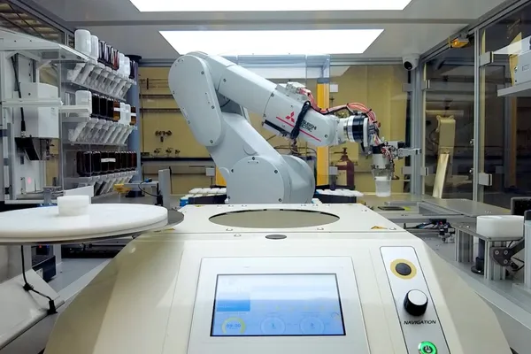
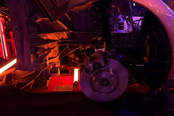
The Idiot Index: How Elon Musk Uses First-Principles Engineering to Cut Costs from Raptor to Cybercab
Explore how Elon Musk applies the "idiot index" to slash manufacturing costs, from SpaceX's Raptor engine to Tesla's rare-earth-free Cybercab drive unit.
read moreInside the Package Optical Engine: Architecture, Packaging, and Physical Limits
Explore the internal architecture of package optical engines: PIC-EIC stacking, micro-ring modulation, fiber coupling, and external InP laser integration.
read more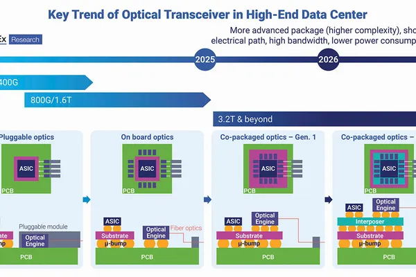
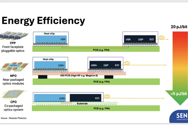
Co-Packaged Optics and the Industrial Bottlenecks of Rack-Scale AI Interconnects
Explore how co-packaged optics (CPO) replaces copper in AI server racks, the packaging challenges of silicon photonics, and critical InP laser supply bottlenecks.
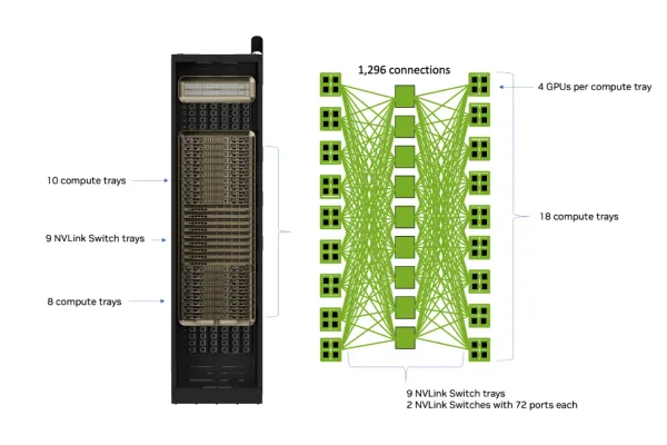
read moreInside NVLink Rack Fabrics: Why Copper Still Dominates AI Scale-Up Over Optics
Discover how NVLink switch silicon and high-density copper fabrics power NVL72-class AI racks, why passive copper beats optics inside the rack, and what limits scale-up domains.
read more