Inside the 800G and 1.6T Optical Transceiver Bottleneck: InP, AI Fabrics, and Geopolitics
- David Rogers
- AI Buildout Supply Chain
- 2026-09-21
NEED TO KNOW
- The Foundational Role of InP: Optical transceivers at 800G and 1.6T require indium phosphide (InP) because silicon cannot efficiently emit light at the 1310 nm (O-band) and 1550 nm (C-band) wavelengths standard in AI optical fabrics.
- Core Manufacturing Bottlenecks: Growth constraints reside in high-purity InP crystal boules, wafer epitaxy yield, and qualified 200G/lane electro-absorption modulated lasers (EMLs).
- Demand Outpacing Capacity: Transceiver demand runs approximately 30% ahead of qualified supply, with 800G+ shipments scaling past 60 million units in 2026, driven primarily by hyperscale AI clusters (Nvidia, Google, Microsoft, Amazon, Meta).
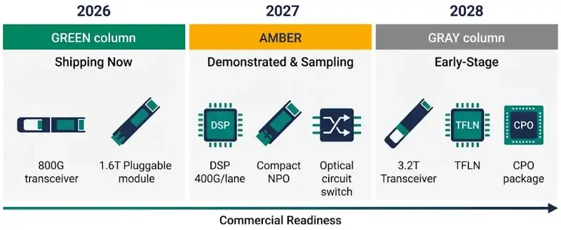
- Power and Architecture Shifts: The industry is transitioning from 2-inch to 6-inch InP wafers, adopting silicon photonics with external continuous-wave (CW) lasers, and evaluating linear pluggable optics (LPO) to reduce DSP power consumption before co-packaged optics (CPO) scales.
- Material and Substrate Concentration: Raw indium is largely a byproduct of zinc refining, with China refining roughly 70% of global supply; polished merchant InP wafers are heavily concentrated among Sumitomo Electric, AXT (Beijing Tongmei), and JX Advanced Metals.
- Geopolitical Interdependence: Global production splits across Western DSPs/lasers (Broadcom, Marvell, Lumentum, Coherent), Japanese/Chinese substrates, and Chinese/Southeast Asian module assembly (InnoLight, Eoptolink, Fabrinet), creating mutual supply-chain exposure under tightening trade controls.
- Unviable Post-Consumer Recycling: Indium recovery from retired transceivers is thermodynamically and economically impractical because individual modules contain only sub-milligram amounts locked in covalent III–V semiconductor matrices.
An 800G or 1.6T pluggable optical transceiver, typically a Quad Small Form-factor Pluggable Double Density (QSFP-DD) or Octal Small Form-factor Pluggable (OSFP) module, converts electrical signals from a GPU or network switch into pulses of light and back again. The primary engineering challenge fits inside a housing the size of a thumb drive: indium phosphide (InP) lasers and light detectors grown layer by atomic layer on high-purity InP wafers; silicon-photonics modulators from chip foundries like TSMC, GlobalFoundries, and Tower; digital signal processors (DSPs) from Broadcom and Marvell built on advanced silicon nodes; and driver chips, all aligned to optical fibers with sub-micron accuracy in cleanrooms. InP remains the only commercial material that efficiently emits light at the 1310 nm and 1550 nm wavelengths used by AI networks. Because pure silicon cannot emit this light effectively, even “silicon photonics” transceivers must attach an external InP continuous-wave laser /Intel USPTO/. Crystal quality, wafer yield, and qualified 200-gigabit-per-second electro-absorption modulated lasers (EMLs) remain the strict manufacturing hurdle that the rest of the industry cannot bypass.
The true supply bottleneck is not final module assembly, but the limited capacity to grow and test qualified compound semiconductors. The tightest shortages are in 200G-per-lane EMLs and raw InP wafers; Lumentum produces the largest share of these 200G lasers /TrendForce/. To resolve this pinch, manufacturers are transitioning InP wafer diameters from 2 inches to 6 inches /Coherent/, signing multi-year supply contracts, moving some designs from discrete EMLs to silicon photonics paired with continuous-wave lasers, and reducing module power through linear optics designs that remove the internal DSP. Co-packaged optics, which mounts optics directly next to the compute chip, remains the long-term solution for power and density, but standard pluggable modules will handle the bulk of network traffic through 2026 and 2027 /Hengtong/. Attaching optical fibers with sub-micron precision and testing lasers under electrical stress remain delicate processes; specialized contract manufacturers like Fabrinet treat this high-precision assembly as a technical barrier to entry rather than standard board mounting /Fabrinet/.
AI training and inference networks run by Nvidia, Amazon, Google, Meta, and Microsoft drive almost all current demand, while Coherent 800ZR and 1.6T ZR modules connect facilities across metro distances /OIF/. Total shipments of approximately 150 million 800G-and-above optical transceivers are expected in 2026 and 2027 /Yole/. Suppliers such as InnoLight, Eoptolink, Coherent, and Lumentum are already shipping 1.6T transceivers in volume, with production backlogs extending into 2027. Traditional telecommunications carriers and corporate enterprise buyers must wait behind hyperscale cloud operators for module allocations.
Factories can expand module assembly much faster than suppliers can produce raw crystal substrates. Most raw indium is extracted as a byproduct of zinc smelting, with China refining roughly 70% of global output. Production of polished InP wafers is concentrated among three primary suppliers: Sumitomo Electric, AXT (through its Chinese subsidiary Beijing Tongmei), and JX Advanced Metals, which collectively supply most of the commercial market. Following export restrictions and licensing rules introduced by China, prices for 6-inch wafers have increased /Nikkei/, prompting companies like AXT, Lumentum, and Coherent to secure capacity with substantial prepayments.
The manufacturing landscape is split between East and West. Chinese manufacturers InnoLight and Eoptolink build the majority of finished 800G and 1.6T modules, supplying a substantial share of Nvidia’s optical transceivers /PhotonCap/, while Coherent, Lumentum, Accelink, Molex, and Applied Optoelectronics provide the remainder. Upstream laser manufacturing remains concentrated at Lumentum, Coherent, Broadcom, Sumitomo, and Mitsubishi; high-speed DSP development belongs mainly to Broadcom and Marvell (alongside Credo and other suppliers working on linear interfaces). Most final assembly takes place in China and Thailand. This split creates clear geopolitical exposure: Western cloud operators rely on Chinese module assembly at scale; Chinese module assemblers require Western DSPs, advanced lasers, and global customers; and every participant requires Japanese or tightly controlled Chinese InP wafers. Regulatory moves by the United States to restrict Chinese optical modules and export controls from China on critical minerals apply conflicting pressures to the same component bill of materials. Nvidia’s multi-billion-dollar supply reservations with Lumentum /NVIDIA/, Coherent /NVIDIA/, and Corning /NVIDIA/ serve to guarantee near-term inventory rather than eliminate these global interdependencies.
Key Insights
What volume or attach-rate of 1.6T transceivers does a next-generation rack architecture like NVIDIA's Vera Rubin NVL72 require?
In an NVIDIA Vera Rubin NVL72 or Rubin Ultra cluster, the transition to 224G SerDes per lane makes 1.6T (OSFP224/OSFP-XD) the foundational optical interconnect tier. While intra-rack GPU-to-GPU scale-up relies on passive copper backplanes and NVLink copper spines across the 72 Rubin GPUs, scale-out networking—via ConnectX-9 SuperNICs running at 1.6 Tb/s and Quantum-X800/X1600 or Spectrum-X switches—mandates high optical attach rates. A fully deployed, three-tier non-blocking fat-tree cluster requires an optical transceiver-to-GPU multiplier between 2.5× and 5×, translating to roughly 200 to over 350 equivalent 1.6T optical modules per NVL72 rack. When scaled to multi-rack clusters (such as the Rubin NVL576 pod spanning 8 racks), inter-rack scale-up and scale-out demand compounds into several thousand 1.6T transceivers per computing unit, cementing optical modules as one of the largest single networking bill-of-materials expenditures in next-generation AI infrastructure.
What is the most critical bottleneck process technology across the 1.6T transceiver manufacturing chain?
The defining physical bottleneck is the epitaxial crystal growth and high-temperature stress screening of 200G-per-lane Electro-absorption Modulated Lasers (EMLs) on Indium Phosphide (InP) substrates. Fabricating a monolithic EML that maintains a >60 GHz electro-optic 3 dB bandwidth across the O-band requires precise control of nanometer-scale InGaAsP/InGaAlAs multi-quantum wells via Metal-Organic Chemical Vapor Deposition (MOCVD) to leverage the Quantum-Confined Stark Effect without introducing carrier-trapping lattice defects. Unlike silicon CMOS fabs that achieve rapid throughput on 300 mm wafers, InP boules grown via Vertical Gradient Freeze (VGF) yield brittle, small-diameter wafers (predominantly transitioning from 2-inch to 6-inch) that suffer from high etch-pit densities, radial dopant non-uniformity, and wafer warping. Combined with the mandatory multi-week burn-in required to weed out infant mortality caused by Dark-Line Defects (DLDs), qualified 200G EML capacity cannot scale linearly with assembly, keeping component lead times stretched across the industry.
How do long-term supply agreements and cyclicality shape the unit economics and margin defensibility of optical component makers?
The unit economics of high-speed optical transceivers are characterized by steep initial gross margins that face structural cyclicality, forcing vendors into capital-intensive multi-year supply lockups. Upstream laser and substrate makers (such as Lumentum, Coherent, and AXT) possess the widest economic moats; 200G EMLs command average selling prices (ASPs) roughly 2× higher than 100G dies against only modest incremental wafer costs, driving non-GAAP gross margins above 40–50% for qualified laser fabs operating at capacity. However, because merchant optical modules face historical price-erosion curves of 15–25% annually once secondary sources ramp, hyperscalers and system integrators (including NVIDIA and cloud titans) increasingly deploy multi-billion-dollar long-term supply agreements (LTAs) and non-cancellable capacity reservations to secure laser allocation. These LTAs smooth the traditional feast-or-famine telecom cycle for compound semiconductor suppliers, shielding upstream fabs from sudden inventory corrections while establishing defensible margin profiles that downstream box assemblers operating on tighter mid-20% gross margins cannot match.