Understanding Semiconductor Etch Machinery: Dry vs. Wet Processes in Advanced Chipmaking
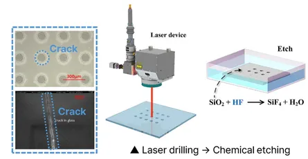
Explore how dry plasma and wet chemical etch machinery shape advanced semiconductor manufacturing, overcoming 2nm fabrication challenges and supply chain risks.
Discover how thin-film deposition (CVD, PVD, and ALD) powers AI hardware. Explore growth trends, top equipment suppliers, and sub-nanometer fabrication advances.
Discover the physics and engineering behind EUV lithography, from 13.5 nm laser-produced plasma and Zeiss optics to High-NA roadmaps and global supply chains.
Discover why DUV lithography remains essential for semiconductor manufacturing. Learn how ASML immersion tools, multi-patterning, and hybrid scaling drive AI chip production.
Discover how Nanoimprint Lithography (NIL) enables low-cost, high-resolution photonics for AI data centers and silicon PICs. Explore Canon’s FPA-1200NZ2C, manufacturing challenges, market demand, and why NIL complements EUV in the AI semiconductor boom. Essential insights on process, firms, and future capacity.