CD-SEM Metrology: Principles, Challenges, and Market Dynamics
- David Rogers
- AI Buildout Supply Chain
- 2026-07-27
NEED TO KNOW
- Primary Function: CD-SEM uses low-energy electron beams (≤ 1 keV) to perform top-down, sub-nanometer linewidth and line-edge roughness (LER/LWR) measurements on semiconductor wafers.
- Core Technological Challenges: Managing lower contrast from ultra-thin EUV resists, mitigating beam-induced sample shrinkage, avoiding surface charging distortion, and imaging 3D structures like GAA nanosheets.
- Key Market Leaders: Hitachi High-Tech dominates the market (60–70%+ share with its CG Series), followed by Applied Materials with its VeritySEM platform.
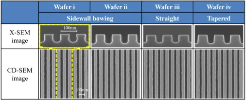
Dimensional metrology measures the physical dimensions of semiconductor features during manufacturing. These measurements include line width, spacing, layer alignment, film thickness, and surface roughness. Operators use this data to keep process steps within narrow manufacturing limits. Engineers use several measurement tools, including optical, atomic force, and X-ray systems. However, Critical Dimension Scanning Electron Microscopy (CD-SEM) is the main tool to image features from above with high resolution /Hitachi High-Tech/. A CD-SEM system operates in a vacuum. It fires a low-energy electron beam (usually less than or equal to 1keV) at the sample surface. This beam produces secondary electrons to create images. Automatic software algorithms then calculate dimension data from these images with sub-nanometer accuracy and high repeatability /ISO/. Production CD-SEM tools operate fully automatically from cassette to cassette, processing an entire batch of silicon wafers completely automatically from start to finish without any human touching or directly handling the individual wafers. Manufacturers design these tools to process wafers quickly in cleanrooms, maintain stable magnification, and prevent sample damage /Applied Materials/.
CD-SEM Electron Beam Measurement Process
High-Vacuum Wafer Loading
Vacuum Chamber IsolationLoad silicon wafer into ultra-high vacuum chamber to eliminate air molecule electron scattering.
Low-Energy Electron Emission
Cold Field Emission GunEmit low-energy electron beam (300eV–1kV) to prevent radiation damage to delicate photoresist features.
Electromagnetic Lens Scanning
Beam Spot FocusingFocus electron beam into sub-nanometer spot size and scan across wafer feature edges.
Secondary Electron Capture
Detector Signal ProcessingCollect emitted secondary electrons at feature edges with high-speed secondary electron detectors.
Sub-Nanometer Width Calculation
AI Edge Profile AnalysisAnalyze electron intensity signal profiles to measure critical dimension widths with sub-0.1nm precision.
Key technical challenges center on maintaining signal quality and measurement fidelity as features shrink below 5 nm and structures become more three-dimensional /Semiconductor Engineering/. Stochastic effects from EUV lithography increase roughness that must be quantified accurately; thinner resists and complex profiles reduce contrast; beam-induced charging, contamination, or shrinkage can distort results; and throughput must stay high enough for statistical process control across entire wafers. Emerging approaches include multi-detector or multi-energy imaging, advanced edge-detection algorithms and machine learning /IEEE/ for faster, more robust analysis, and hybrid workflows that combine limited CD-SEM data with optical or X-ray measurements to reduce reliance on slower or destructive methods.
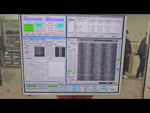
Demand is tightly linked to the expansion of advanced logic (GAA and beyond), high-bandwidth memory, 3D NAND, and packaging lines, where precise CD and roughness control directly determine yield and device performance. Overall, Hitachi High-Tech (Japan) is the long-standing market leader in CD-SEM, with its CG-series platforms historically commanding dominant shares (often cited in the 60–70 % range) /Market Growth Reports/. Applied Materials (United States) holds a meaningful secondary position with its Veritas systems, while Thermo Fisher, JEOL, and others serve specialized or research segments. CD-SEM tools are capital equipment that are typically upgraded or refurbished over long service lives /Wiley/.
Key Insights
What is the estimated CD-SEM tool install base and volume demand for leading-edge processes like TSMC N2, Intel 14A, or SK Hynix 1c/HBM4E?
A typical mega-fab module running 50,000 wafer-starts-per-month (WSPM) at advanced nodes like TSMC N2 or Intel 14A requires an install base of roughly 40 to 60 dedicated CD-SEM tools to support high sampling intensity across multi-patterning lithography, etch, and CMP steps. In advanced memory lines like SK Hynix 1c DRAM and HBM4E base-die fabrication, tool density ranges between 20 and 35 units per 50k WSPM, driven by strict pitch-walking checks and micro-bump dimensioning. Given high-volume manufacturing (HVM) rollouts across global fabs, the industry-wide annual demand for leading-edge production CD-SEMs hovers around 250 to 350 new units annually, expanding total global active install bases in advanced fabs to several thousand systems.
What is the most critical process technology bottleneck in modern CD-SEM equipment?
The absolute performance bottleneck in sub-2 nm CD-SEM design lies in electron beam physics and high-speed detection: specifically, optimizing low-energy electron optics to achieve sub-nanometer spatial resolution without destroying fragile, ultra-thin EUV photoresists or inducing line shrinkage. Generating sufficient signal-to-noise ratio (SNR) at low landing energies (≤ 500 eV) requires high-brightness Schottky field-emission guns paired with aberration-corrected electrostatic-magnetic objective lenses. In tandem, ultrafast secondary-electron and backscattered-electron detectors must capture multi-angle topographic signals at high frame rates to maintain throughput while extracting complex 3D profiles in gate-all-around (GAA) nanosheets and high-aspect-ratio memory holes.
What are the unit economics, pricing structures, and margin dynamics of CD-SEM tools?
CD-SEM equipment commands high unit economics, with flagship production platforms (such as Hitachi's CG series or Applied Materials' VeritySEM) carrying average selling prices (ASPs) ranging from $4 million to over $8 million per tool depending on multi-detector configurations and software automation packages. Due to high engineering barriers and market concentration between Japan and the U.S., vendors enjoy gross margins of 50% to 60%+, fortified by long-term service agreements (LTSAs) that yield predictable, high-margin software updates, calibration services, and field upgrades over 10- to 15-year tool lifetimes. While tool shipments track overall fab equipment capital expenditure cycles, the growing metrology intensity per wafer at sub-2 nm nodes provides structural margin defensibility and insulates CD-SEM leaders from severe cyclical downturns.