Optical Semiconductor Metrology: Physics, Market & AI Innovations
- David Rogers
- AI Buildout Supply Chain
- 2026-07-27
NEED TO KNOW
- Essential Light Sources & Physics: Leading-edge inspection relies on Laser-Sustained Broadband Plasma (DUV-to-visible), scatterometry, ellipsometry, and 13.5 nm actinic EUV paired with CaF₂ catadioptric optics to achieve sub-nanometer sensitivity.
- Overcoming Physics Limits with AI: Advanced physics-informed neural networks (PINNs) and surrogate models accelerate inverse spectral prediction by >100×, bypassing optical diffraction limits in sub-5 nm nodes and high-aspect-ratio (HAR) structures without destructive sampling.
- Virtual Metrology & AI Smart Sampling: Innovators like Gauss Labs (Panoptes VM), Tignis (acquired by Cohu), and Averroes AI use real-time sensor telemetry and physics-informed ML to predict wafer outcomes across 100% of wafers, bypassing physical sampling bottlenecks.
- Market Dynamics & Spend: The global process-control and metrology equipment market reached >$18B (14% of Wafer Fab Equipment spend) and is projected to scale to ~$25B by 2031, driven by GAA, High-NA EUV, and advanced packaging.
- Competitive & Geopolitical Concentration: KLA dominates overall yield management with a 55–60%+ market share, while Japan's Lasertec holds a near-total monopoly on actinic EUV mask inspection—making these tools critical geopolitical chokepoints amid global export controls.
Optical metrology and inspection systems use light to measure microscopic semiconductor features during chip manufacturing. Specialized inspection tools use deep ultraviolet plasma and laser scatterometers to scan silicon wafers without damaging them /NIST/. Precision lenses made from calcium fluoride (CaF₂) focus the light beams onto wafer surfaces. High-speed optical sensors measure feature widths, layer alignment, and surface defects with sub-nanometer precision. Foundries use this real-time measurement data to detect manufacturing errors and maintain high wafer yields.
Optical Scatterometry & Defect Inspection Process
Automated Wafer Alignment
Precision Chuck PositioningLoad a silicon wafer onto a vibration-isolated stage and position target measurement sites precisely.
DUV Laser Light Illumination
Beam ProjectionProject deep ultraviolet plasma or laser light beams through precision glass optics onto the wafer surface.
Diffracted Light Collection
Spectral Data CaptureMeasure reflected light intensity, color shifts, and polarization angles using high-speed optical sensors.
AI Signal Reconstruction
3D Profile CalculationAnalyze diffracted light patterns with physics-informed neural network software to calculate sub-nanometer feature dimensions.
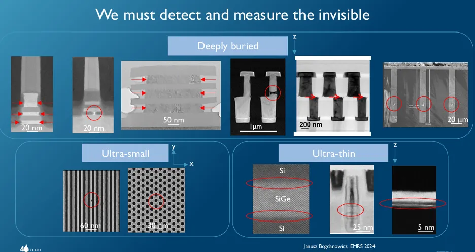
Key technical challenges arise as devices scale into the angstrom era and 3D architectures: optical diffraction and near-field effects degrade signal-to-noise for sub-5 nm features; high-aspect-ratio (HAR) structures in 3D NAND or TSVs (>50:1, approaching 100:1) cause severe light attenuation and parameter coupling /SPIE/; buried defects in hybrid bonding and GAA transistors evade surface inspection; and tool-to-tool matching plus process variations complicate consistency. Emerging solutions center on AI-driven hybrid metrology using physics-informed neural networks /SPIE/, surrogate models for inverse spectral prediction, and multi-modal data fusion that deliver >100× throughput gains, sub-nm accuracy, and reduced reliance on slow or destructive e-beam/X-ray methods, while cutting waste through better first-pass yield and fewer discarded wafers.
The Rise of Virtual Metrology (VM) & Smart Sampling
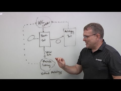
To overcome the physical throughput limitations of hardware metrology tools—which sample only 1% to 5% of processed wafers—the semiconductor industry is rapidly adopting Virtual Metrology (VM) /Semiconductor Engineering/. Virtual Metrology utilizes real-time equipment sensor telemetry (Fault Detection and Classification / FDC data, including chamber pressures, gas flow rates, plasma spectra, and RF power) paired with advanced machine learning models to predict physical wafer properties (film thickness, critical dimensions, and overlay) for 100% of wafers in real time.
Industry leaders and technical approaches in Virtual Metrology include:
- Gauss Labs: An industrial AI pioneer (backed by SK Hynix) leading commercial Virtual Metrology deployment with its Panoptes VM platform /Gauss Labs/. Deployed across SK Hynix DRAM and NAND high-volume manufacturing lines, Panoptes VM expands wafer coverage from limited physical sampling to near-100% virtual monitoring, achieving up to a 29% reduction in process variance.
- Tignis (Acquired by Cohu): Develops PAICe Maker, a physics-driven AI platform that embeds virtual metrology directly into Advanced Process Control (APC) systems /Cohu/. Tignis’s hybrid approach combines physical domain models with machine learning to enable real-time, wafer-to-wafer recipe adjustments and intelligent “smart sampling” for physical metrology tools.
- Averroes AI: Offers AI-powered visual inspection and virtual metrology software /Averroes AI/ that integrates with fab APC infrastructure to predict physical film and etching parameters, cutting physical sampling overhead, preventing excursion cascades, and accelerating yield learning ramps.
End-use demand is surging with AI accelerators, high-bandwidth memory, advanced packaging (hybrid bonding, chiplets), high-NA EUV, and GAA transistors, which intensify process-control needs across front-end wafer fabs and back-end assembly. The overall metrology and inspection equipment market surpassed $18 billion in 2025 (about 14% of wafer fab equipment spend) and is projected to reach roughly $25 billion by 2031 /Yole/, with optical systems forming the largest share as process-control intensity rises faster than capacity expansion itself.

Production capacity is constrained by the extreme specialization of these tools. KLA alone has installed roughly 3,000 broadband plasma systems historically /KLA/, yet lead times remain long and output is gated by precision optics, sensors, and cleanroom assembly. Thus, KLA dominates with 55–60%+ overall process-control share and near-sole-source status for high-end optical wafer inspection and overlay; Lasertec (Japan) holds a monopoly on actinic EUV mask inspection essential for printable defect detection /Lasertec/; other key players include ASML/Zeiss (mask and optics metrology), Hitachi High-Tech, Onto Innovation, Nova, and Applied Materials. Geopolitical concentration risks are acute as the U.S. and Japanese export controls restrict advanced tools to China, creating parallel ecosystems and potential chokepoints that can delay yield ramps at every leading-edge fab worldwide.
Key Insights
What is the estimated volume or installed base of broadband plasma metrology systems in a leading-edge fab (e.g., TSMC N2, Intel 14A, or SK Hynix HBM4)?
A single leading-edge megafab module—such as those powering TSMC’s N2, Intel’s 14A, or SK Hynix’s 1c DRAM/HBM4 lines—typically deploys between 80 and 120 total inspection and metrology tools, with high-sensitivity Broadband Plasma (BBP) optical defect inspection tools representing 15 to 25 flagship units per fab phase. Because GAA nanosheets and high-aspect-ratio 3D structures require far more non-destructive sampling passes per wafer, BBP tool intensity rises rapidly at sub-2 nm nodes. Historically, single vendors like KLA have accumulated a global installed base of roughly 3,000 BBP systems, but new leading-edge fabs require continuous additions to prevent yield learning bottlenecks.
What is the most critical bottleneck process technology in optical metrology equipment production?
The primary production bottleneck for optical metrology tools is the fabrication, coating, and active alignment of ultra-high-purity catadioptric optics (utilizing defect-free Calcium Fluoride (CaF₂) crystals) alongside high-radiance Laser-Sustained Plasma (LSP) light source assemblies. Unlike standard commercial equipment, these optical components must resist compaction and solarization damage under continuous DUV radiation while operating near Abbe’s diffraction limit. Because these specialized optical trains and ultra-low-expansion mirror assemblies depend on a highly concentrated supply chain (dominated by Carl Zeiss and specialized lens fabricators), tool production cannot be rapidly scaled by merely increasing raw cleanroom assembly footprint.
What are the unit economics, pricing, and margin defensibility of broadband plasma optical tools?
Flagship Broadband Plasma wafer inspection tools command premium average selling prices (ASPs) ranging from $20 million to over $30 million per system, enabling market leaders like KLA to maintain gross margins near 60–65% and structural operating margins exceeding 40%. The unit economics are reinforced by long-term service agreements (LTSAs) tied to a massive installed base, which generates high-margin recurring software updates, laser source refurbishments, and optics replacements across multi-year semiconductor cycles. Because catastrophic yield excursions on advanced wafers cost foundries millions of dollars per batch, process-control tools act as 'yield insurance,' granting vendors immense pricing power and strong economic moats that insulate them during broader industry downcycles.
What is Virtual Metrology (VM) and how does AI enable 100% wafer monitoring in semiconductor fabs?
Virtual Metrology (VM) is an AI-driven technique that uses real-time equipment sensor data (such as chamber pressure, gas flows, and plasma spectra) combined with machine learning to predict wafer physical parameters (film thickness, critical dimensions, and overlay) for 100% of wafers without physical tool sampling. Leading VM providers include Gauss Labs (with its Panoptes VM deployed at SK Hynix), Tignis (acquired by Cohu, providing physics-driven PAICe Maker platforms for closed-loop APC), and Averroes AI. Virtual metrology enables smart sampling, reduces process variance by up to ~30%, and cuts expensive physical metrology bottlenecks in sub-3nm nodes.