The Unsung Workhorse: Why DUV Lithography Still Powers the Chip Industry
- David Rogers
- AI Buildout Supply Chain
- 2026-07-21
NEED TO KNOW
- The Foundation of Hybrid Scaling: EUV targets the smallest layers, but DUV (ArFi/KrF) patterns 2–3x more layers per wafer in modern sub-3nm chip stacks.
- Economic Workhorse: ASML’s TWINSCAN NXT immersion tools achieve throughputs exceeding 6,000 wafers/day, delivering low cost-per-layer efficiency.
- Broad Market Demand: Essential for mature nodes (≥ 28nm), automotive, IoT, power electronics, and 3D NAND/HBM memory production.
- Market Leader: ASML holds 85–90% of advanced DUV immersion share, complemented by Nikon and Canon.
- China’s Homegrown Immersion Ramp: Shanghai Aishengna has consolidated R&D from Yuliangsheng and SMEE to initiate mass production of domestic immersion DUV scanners (targeting 5 units in 2026 and 20 in 2027).
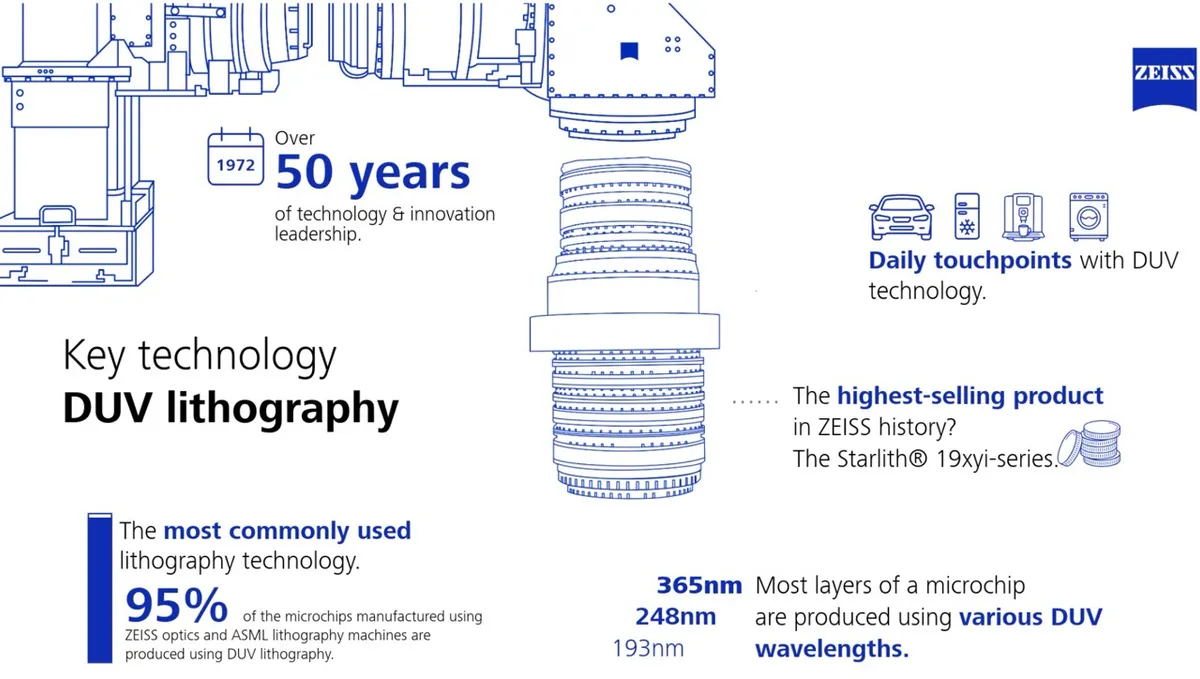
Deep ultraviolet (DUV) lithography machines use laser light to print circuit patterns on the majority of semiconductor layers /EETimes/. DUV systems use 193 nm and 248 nm laser wavelengths paired with high-precision glass lenses. While extreme ultraviolet (EUV) tools print the smallest microchip features, DUV systems print most of the remaining circuit layers. High-throughput DUV scanners process over 6,000 silicon wafers per day in high-volume chip foundries.
Here is how specific models in the NXT series perform /ASML/:
- TWINSCAN NXT:1980Fi: Reaches up to 330 wafers per hour (approx. 7,920 theoretically).
- TWINSCAN NXT:2050i: Produces 295 wafers per hour, capable of 4,600+ wafers per day.
- TWINSCAN NXT:2000i: Achieves a champion productivity of 4,600 wafers per day natively, with records of over 6,300 exposed in a single day by customers.
DUV Immersion Lithography Exposure Cycle
Wafer Loading & Immersion Injection
Water Layer DispensingLoad a 300mm silicon wafer onto the stage and inject pure deionized water into the space below the lens.
193nm Laser Emission
Excimer Light GenerationFire high-speed 193nm argon fluoride excimer laser pulses through a circuit pattern photomask reticle.
Catadioptric Lens Reduction
Sub-Nanometer Optical FocusingFocus light through specialized Carl Zeiss CaF₂ glass lenses to shrink circuit patterns four times smaller.
Dual-Stage Wafer Scanning
TWINSCAN High-Speed ExposureScan the wafer under the laser beam at high acceleration across TWINSCAN dual stage platforms.
Water Extraction & Post-Bake
Photoresist Pattern FixationExtract the water layer rapidly from the wafer surface and perform post-exposure baking to fix circuit patterns.
Key challenges include sustaining yield and cost amid multi-patterning complexity, line-edge roughness, and defect control, especially as nodes push limits with existing tools. Emerging optimizations target higher throughput, better cross-matching with EUV layers /ASML/, improved resists (e.g., reduced clustering via process tweaks like post-exposure bake), and sustainability in materials/chemicals. While not as glamorous as EUV, DUV’s reliability and lower cost per layer make it indispensable creating 2-3x more layers per wafer than EUV in hybrid flows.
Demand is robust and growing for mature-node capacity in automotive, IoT, power, analog, and RF chips, plus support for leading-edge logic production. Global semiconductor expansion, AI-driven memory needs, and government fab incentives (e.g., CHIPS Acts) drive wafer starts, with DUV handling mainstream and non-critical layers. Market projections show steady growth through 2030+, fueled by geographic diversification of semiconductor fabrication /Mordor Intelligence/.
ASML holds ~85-90% of advanced DUV immersion share globally, with Nikon and Canon serving mature/specialty segments. However, tightening Western export controls limiting advanced DUV immersion tool shipments to China have dramatically accelerated Chinese self-sufficiency efforts /Congress/.
The trajectory of domestic Chinese DUV technology reflects a multi-stage industrial evolution across three key entities:
- Shanghai Micro Electronics Equipment (SMEE): As China’s legacy lithography champion, SMEE established the foundational R&D baseline for dry DUV (600 series scanners for 90nm/28nm dry nodes) and initial immersion optics and stage components, though scaling to high-yield immersion mass production independently proved challenging.
- Shanghai Yuliangsheng Technology: Operating as a startup affiliate within the Huawei-backed SiCarrier semiconductor equipment coalition, Yuliangsheng spearheaded prototype immersion DUV scanner development. In late 2025, Yuliangsheng successfully initiated fab-level testing of domestic immersion scanners at SMIC, validating core sub-systems.
- Shanghai Aishengna Electronic Technology Group: Established in August 2023 with 7 billion RMB (~$1 billion) in capital backed by Shanghai Electric, Aishengna emerged in mid-2026 as the consolidated national champion. By absorbing engineering teams, patents, and operational assets from both Yuliangsheng and SMEE, Aishengna has unified China’s immersion DUV effort into a single mass-production entity.
In July 2026, Aishengna officially initiated mass production of homegrown immersion DUV scanners, targeting an initial delivery volume of 5 units in 2026 and scaling to 20 units in 2027 for major domestic chipmakers including SMIC, Hua Hong Semiconductor, and ChangXin Memory Technologies (CXMT) /Reuters/. Capable of native single-exposure resolutions around 28nm, these tools can achieve sub-7nm pattern features when paired with aggressive multi-patterning techniques (SADP/SAQP). While these domestic immersion scanners remain several generations behind ASML’s latest TWINSCAN NXT platforms in throughput, overlay matching, and sub-component maturity, their commercial deployment represents a landmark milestone in establishing an independent domestic semiconductor manufacturing stack. Installed bases globally remain massive (>1,300 immersion systems), with strong recycling/upgrades extending tool life while regional ecosystems bifurcate.
In summary, DUV lithography remains a vital pillar of semiconductor manufacturing rather than a legacy technology. Its evolution through advanced immersion systems (ArFi), multi-patterning integration (SADP/SAQP), and precise EUV cross-matching ensures high-volume yield and cost performance across logic and memory stacks. DUV’s operational reliability, cost-per-layer efficiency, and expanding global footprint make it essential for sustaining the physical and economic momentum of the global electronics ecosystem.
Key Insights
How many lithography layers are typically patterned with DUV versus EUV in advanced 3nm or 2nm logic processes?
A modern 3nm or 2nm logic process stack comprises 60 to 90+ total lithography masking steps. EUV is selectively deployed for 10 to 20 critical, dense layers, leaving 40 to 70+ layers to be processed by DUV (ArFi and KrF), yielding a 2x–3x ratio.
What is the install base and volume estimate for DUV lithography tools in semiconductor fabs?
DUV lithography systems, particularly ASML’s TWINSCAN NXT immersion scanners, form the backbone of semiconductor production with over 1,300 high-end immersion tools installed globally, handling the majority of wafer layers even in advanced AI accelerators like NVIDIA’s Vera Rubin. In leading-edge fabs (TSMC, Samsung, Intel), DUV tools pattern 2–3 times more layers than EUV per wafer, supporting high-volume mature-node capacity expansions critical for HBM, packaging, and support structures in AI GPUs. Annual shipments continue strongly alongside EUV ramp, with productivity upgrades enabling thousands of wafers per day per tool to meet surging AI-driven demand.
What is the most critical bottleneck process technology in DUV lithography for mature nodes?
The most critical bottleneck in DUV lithography remains multi-patterning complexity (SADP/SAQP) combined with overlay precision, line-edge roughness, and defect control when pushing mature nodes or non-critical layers in advanced processes. While tools like ASML NXT:2100i deliver excellent throughput and matching with EUV, achieving cost-effective yield at scale for high-volume applications requires ongoing advances in photoresist purity, process optimization, and fab-wide integration.
What is the state of China's domestic immersion DUV lithography technology?
In July 2026, China officially transitioned to mass production of domestic immersion DUV scanners under Shanghai Aishengna Electronic Technology Group. Aishengna consolidated engineering teams and IP from early lithography pioneer SMEE and Huawei-backed startup Yuliangsheng Technology. With native single-exposure resolution around 28nm, these tools can achieve 7nm/5nm features via multi-patterning. Aishengna targets 5 scanners in 2026 and 20 in 2027 for SMIC, Hua Hong, and CXMT, providing a critical domestic alternative to restricted ASML NXT immersion tools.
What are the unit economics, long-term supply agreements, cyclicality, and margin growth/defensibility for DUV lithography systems?
DUV lithography systems offer strong unit economics through high utilization, service annuities (growing >30%), and upgrade packages on a massive installed base, with ASML leveraging AI-driven demand and supply constraints to pursue price increases despite TSMC’s pushback on broader capex pressures. Long-term supply agreements with major foundries provide visibility amid cyclicality, while robust memory/logic demand, capacity expansions, and ASML’s bottleneck positioning support margin growth and defensibility as the AI buildout drives higher overall costs for semiconductor manufacturing.