Nanoimprint Lithography: Patterning the Future of Photonics and Semiconductor Manufacturing
- David Rogers
- AI Buildout Supply Chain
- 2026-07-20
NEED TO KNOW
- Low-Capex, Low-Energy Patterning: Nanoimprint Lithography (NIL) tools cost ~$15–30M (10% of EUV scanners) and consume up to 90% less power by stamping features directly.
- 3D Nanostructure Capability: NIL prints complex 3D, multi-tier nanostructures in a single press, eliminating multi-mask EUV exposure steps for photonic waveguides.
- Template Durability Bottleneck: Physical contact limits quartz template lifetimes to ~50 wafers, driving research into AI-optimized molds and hybrid resists.
- Japan-Centric Ecosystem: Commercial NIL deployment is led by Canon (FPA-1200NZ2C) and Dai Nippon Printing, representing an alternative to ASML's EUV monopoly.
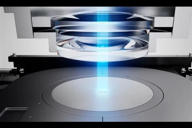
Nanoimprint lithography (NIL) uses a high-precision quartz mold to stamp physical patterns onto semiconductor wafers /IEEE/. A liquid chemical resist fills the mold features before ultraviolet light cures the pattern solid. Because this stamping process eliminates complex projection lenses, it consumes significantly less power than optical lithography scanners. Nanoimprint lithography is especially effective for manufacturing 3D optical components like waveguides and photonics chips for AI data centers.
Nanoimprint Lithography Photonic Pattern Transfer Process
Resist Jet Dispensing
Liquid Droplet GridDispense microscopic droplets of low-viscosity UV resin across a silicon photonic wafer.
Sub-Nanometer Alignment
Quartz Mold PositioningAlign the 3D quartz master mold with sub-nanometer precision over target wafer alignment marks.
UV Light Photocuring
Resist HardeningPress the quartz mold into liquid resin and shine 365nm UV light to polymerize the nanostructures instantly.
Demolding & Anisotropic Etch
3D Waveguide PatterningPull the mold away cleanly and plasma etch the wafer to transfer 3D optical waveguide features for AI interconnects.
Key technical challenges center on mold defectivity, template wear, and overlay alignment. Physical contact means particles on the wafer can damage the expensive quartz mold, creating repeating defects. Current templates last roughly 50 wafer imprints before requiring replacement or cleaning, driving up operational costs. Furthermore, overlay precision (aligning multi-layer patterns) has historically lagged optical scanners. Emerging solutions include AI-driven defect inspection systems, self-cleaning anti-stick coatings, higher-durability diamond-like carbon (DLC) template materials, and adaptive gas-cushion pressing to improve alignment yield.
NIL offers compelling economics. Equipment costs are roughly $15M to $30M per tool—less than 10% of a High-NA EUV scanner—while operating power consumption drops by 90%. Market adoption is accelerating in 3D NAND flash, silicon photonics, co-packaged optics (CPO), and AR/VR optical waveguides where 3D structures are difficult to produce via EUV. Canon’s FPA-1200NZ2C tool represents the primary commercial platform targeting logic nodes down to 2nm, backed by template partnerships with Dai Nippon Printing (DNP). As AI hardware demands denser photonics integration, NIL provides a scalable, energy-efficient alternative to traditional photolithography.
Driven by the rise of AI data centers, demand for NIL is accelerating rapidly in the optical interconnect space. By enabling cost-effective, scalable production of silicon photonics, NIL facilitates high-bandwidth, energy-efficient optical links designed to overcome the physical throughput limitations of traditional copper interconnects. Beyond data centers, the technology underpins advancements in augmented reality optics, high-efficiency LEDs, photovoltaic light-trapping layers, and environmental sensors. Industry analysts project substantial growth for the NIL equipment market, positioning it not as a direct replacement for EUV on leading-edge logic nodes, but as a vital complementary technology for memory layers, back-end interconnects, and specialty photonic devices /Grand View Research/.

On the commercial front, Canon leads the market with its flagship FPA-1200NZ2C system /Canon/, supported by an ecosystem that includes Dai Nippon Printing for templates and materials suppliers like Toyo Gosei, Morphotonics, and Scivax. This grants Japan a concentrated hold on NIL processing technology, presenting lower geopolitical risk than ASML and Zeiss’s EUV monopoly, albeit with its own template supply dependencies. Concurrently, emerging Chinese firms like Prinano have validated mass production for photonic chips using NIL in partnership with Shenzhen Litra Technology and its PL-AS vacuum air-cushion platform /IE/. Even so, near-term equipment capacity growth remains controlled, with market leaders like Canon targeting modest production volumes of 10 to 20 units annually.
Ultimately, nanoimprint lithography offers a compelling, low-power alternative to conventional photolithography by dramatically lowering the cost barrier for complex nanostructures. While overlay and template wear challenges may slow its displacement of EUV in leading-edge logic, its distinct advantages make it uniquely suited for the surging demand in photonics and optical communications /Semiconductor Engineering/. As manufacturing ecosystems mature and AI-driven optimizations refine tool performance, NIL is poised to become a competitive pillar of next-generation optical and semiconductor manufacturing.
Key Insights
What are the main economic advantages of Nanoimprint Lithography (NIL) versus EUV?
NIL offers significant cost-of-ownership advantages over EUV lithography, driven primarily by lower upfront capital expenditure and dramatically reduced energy consumption. NIL tools cost roughly $15–30 million per system—about one-tenth the price of a modern EUV scanner ($150–300+ million) while consuming up to 90% less power to operate. Additionally, its simplified process flow reduces the total tool count and operational steps required in the fab. Recent breakthroughs, such as Dai Nippon Printing’s 10 nm line-width templates designed for 1.4 nm-class nodes, demonstrate that NIL can achieve competitive logic-level resolution at a fraction of EUV's cost. While short template lifespans (currently ~50 wafers) remain a challenge, NIL already delivers superior unit economics for application layers like photonics and memory.
What is the most critical process bottleneck for Nanoimprint Lithography in the AI buildout?
The main operational bottleneck is template durability and defect density caused by the physical contact nature of the imprinting process. In production, mechanical stress, particle contamination, and physical wear limit template lifetimes to roughly 50 wafers—far below the 500+ wafer threshold needed for high-volume logic manufacturing. Secondary challenges include overlay alignment precision (which lags logic requirements by about 4x) and tool throughput (~25 wafers/hour per cell). However, these constraints are significantly less prohibitive for AI-driven photonics and optical interconnects, where complex 3D nanostructures and low manufacturing costs take priority over ultra-dense multilayer alignment.
What are the unit economics of Nanoimprint Lithography machinery, including supply agreements, cyclicality, and margin defensibility?
NIL tools deliver compelling economics by pairing low capital expenditures with minimal material waste from jet-dispensed resists. For equipment vendors like Canon, profitability is anchored by high-margin tool sales, recurring maintenance services, and consumable ecosystem partnerships (e.g., template replication with Dai Nippon Printing). Long-term supply agreements with foundries and memory manufacturers provide steady revenue visibility. Furthermore, NIL exhibits lower cyclicality than leading-edge EUV because its adoption spans diverse growth markets beyond traditional logic, including silicon photonics, optical sensors, and AR displays. Its margin defensibility is fortified by deep process know-how and a tight, Japan-centric concentration of specialized template and material suppliers—though improving template longevity remains the critical variable to maintaining its ~40% cost advantage over deep-UV multi-patterning.