SOI Wafers: The Critical Substrate Powering Silicon Photonics for AI Data Centers
- David Rogers
- AI Buildout Supply Chain
- 2026-07-09
NEED TO KNOW
- Silicon Photonics Foundation: Silicon-On-Insulator (SOI) wafers feature a thin top silicon device layer (220–300nm) over a buried oxide (BOX) layer, delivering optical confinement for high-speed waveguides.
- Smart Cut® Process Dominance: France's Soitec holds a near-monopoly on photonics-grade SOI wafers manufactured via Smart Cut® hydrogen ion implantation, thermal splitting, and CMP polishing.
- Replacing Copper Interconnects: Explosive demand for Co-Packaged Optics (CPO) and 800G/1.6T transceivers is projecting the SiPh market to reach $9B–$28B by 2034.
- US Domestic Diversification: GlobalWafers is expanding 300mm SOI wafer capacity in Missouri via US CHIPS Act funding to reduce sole-source dependence on European facilities.
Silicon-on-insulator (SOI) wafers are specialized silicon disks used to build optical microchips for AI data centers. Each wafer contains a thin top silicon layer separated from the base wafer by a buried oxide insulating layer /UniversityWafer/. The insulating oxide layer traps laser light inside the top silicon layer with minimal signal loss. This structure allows engineers to integrate optical laser components onto silicon chips, replacing copper cables with high-speed light signals.
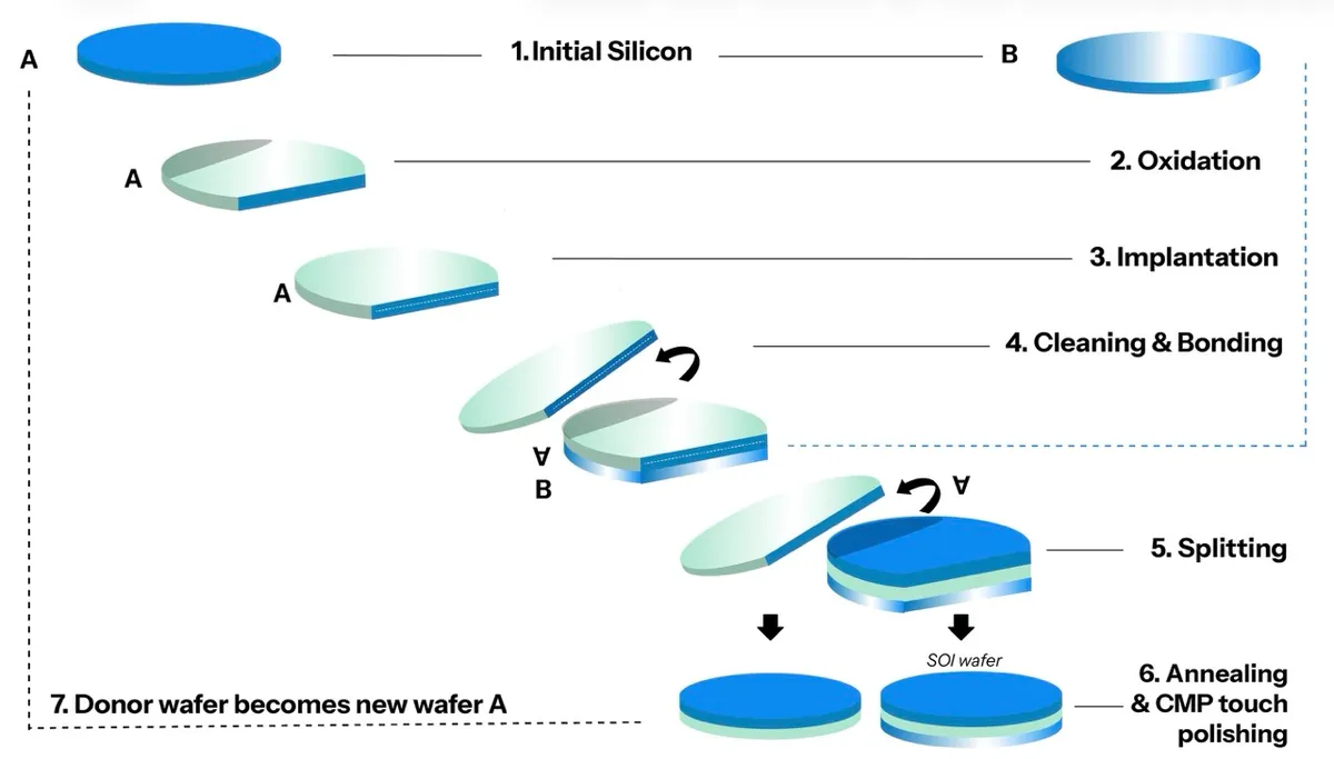
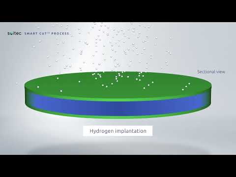
Production relies primarily on Soitec’s proprietary Smart Cut® process (licensed to others), which combines hydrogen ion implantation into a donor wafer, room-temperature hydrophilic bonding to an oxidized handle wafer, controlled thermal splitting to transfer a uniform thin silicon film, and final chemical-mechanical polishing (CMP) plus annealing for surface quality and defect repair /Soitec/. An older alternative, Separation by IMplanted OXygen (SIMOX), uses high-dose oxygen implantation followed by high-temperature annealing to form the buried oxide /ScienceDirect/. Both demand semiconductor-grade purity (sub-ppb metallic impurities, minimal crystal defects) and nanometer-scale uniformity in layer thickness and smoothness are essential for consistent waveguide effective index and minimal scattering losses in photonic circuits.
Smart Cut® Silicon-on-Insulator (SOI) Wafer Process
Oxidation & Hydrogen Implantation
Atomic Marker LayerGrow an oxide layer on a donor silicon wafer and shoot high-energy hydrogen ions to a precise depth.
Hydrophilic Direct Bonding
Wafer AttachmentBond the oxidized donor wafer face-down onto a clean silicon handle wafer at room temperature.
Thermal Cleaving
Thin Film TransferHeat the bonded wafers so micro-bubbles along the hydrogen layer split off a thin silicon film.
Surface Polishing & Annealing
Photonic Surface FinishingPolish and heat-treat the top silicon layer to make an optical waveguide layer for AI photonics chips.
Key challenges include high manufacturing cost and complexity versus bulk silicon wafers: expensive high-energy ion implanters /Axcelis/, stringent particle/void control in bonding, precise splitting mechanics, and material-intensive CMP. Yield and uniformity on 300 mm wafers remain demanding, especially for photonics-grade low-loss performance across large areas. Emerging solutions focus on process optimizations for higher throughput, improved metrology, fungible capacity reallocation across SOI lines /ResearchGate/, and higher-volume ramps to amortize costs. Recycling of donor wafers or reclaim processes offers limited near-term relief due to the layered structure, though general silicon wafer reclaim (etch/polish) provides cost and waste-reduction pathways for test/monitor material.
Explosive demand is driven by silicon photonics for AI infrastructure including co-packaged optics (CPO), pluggable transceivers (800G/1.6T+), and optical fabrics in data centers and HPC /PhotonCap/. The broader silicon photonics market has a wide range of projections to grow from roughly $2.8–3 billion in 2025 to $9–28 billion by 2030–2034 at CAGRs of 23–29%, with AI/cloud workloads as the primary accelerator. Photonics-SOI substrates are the starting material for leading foundry platforms, enabling the power savings (up to 30% in some architectures) and density required as electrical interconnects hit physical limits.
Supply is highly concentrated. Soitec (France) dominates with its Smart Cut IP portfolio and near-monopoly position in photonics-grade SOI at meaningful scale; its Bernin and Singapore facilities support 200/300 mm production /Soitec/, with new tooling underway for 300 mm Photonics-SOI and fungible capacity that can be redirected as CPO/1.6T ramps accelerate (Photonics-SOI revenue already approaching €100 million scale). GlobalWafers (via MEMC in Missouri) is ramping U.S. 300 mm SOI production with CHIPS Act support, creating a key domestic source /NIST/. Shin-Etsu (Japan) also produces licensed SOI.
As AI buildout intensifies optical interconnect deployment, SOI wafer supply, led by Soitec’s technology moat and selective geographic diversification, will be a critical pacing item. Continued yield gains, capacity activation, and strategic inventory management will determine how smoothly the industry scales the photonic layer of the AI stack.
Key Insights
Why are silicon-on-insulator (SOI) wafers used in silicon photonics for AI?
Silicon-on-insulator wafers feature a thin single-crystal silicon layer over a buried oxide layer, providing the optical confinement and electrical isolation needed for high-speed waveguides. This structure allows passive photonic components like modulators and multiplexers to be integrated alongside electronic circuits, enabling energy-efficient optical interconnects in AI data centers.
What is the Smart Cut process used to manufacture SOI wafers?
The Smart Cut process, developed by Soitec, implants hydrogen ions into a donor silicon wafer to create a cleavage plane, bonds the wafer to an oxidized handle substrate at room temperature, and applies heat to split the donor wafer along the implant line. The resulting thin, uniform silicon layer is polished to achieve nanometer-scale flatness.
Which manufacturers supply photonics-grade SOI wafers, and where is production scaling?
Soitec in France holds a near-monopoly on photonics-grade SOI wafers, producing them at facilities in Bernin and Singapore. To diversify the supply chain, GlobalWafers is ramping up 300mm SOI wafer production in Missouri with support from the U.S. CHIPS Act, establishing a critical domestic source for North American fabs.